- 您现在的位置:买卖IC网 > Sheet目录2006 > LTC2446IUHF#TRPBF (Linear Technology)IC ADC 24BIT 8CH HI SPEED 38QFN
LTC2446/LTC2447
3
24467fa
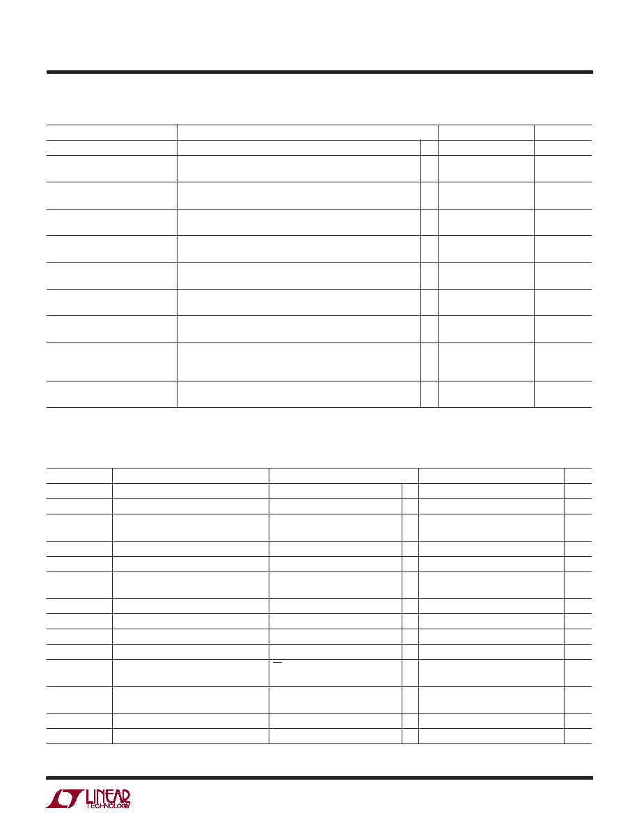
ELECTRICAL CHARACTERISTICS
PARAMETER
CONDITIONS
MIN
TYP
MAX
UNITS
Resolution (No Missing Codes)
0.1V
≤ VREF ≤ VCC, –0.5 VREF ≤ VIN ≤ 0.5 VREF, (Note 5)
●
24
Bits
Integral Nonlinearity
VCC = 5V, REF+ = 5V, REF– = GND, VINCM = 2.5V, (Note 6)
●
5
15
ppm of VREF
REF+ = 2.5V, REF– = GND, VINCM = 1.25V, (Note 6)
3
ppm of VREF
Offset Error
2.5V
≤ REF+ ≤ VCC, REF– = GND,
●
2.5
5
V
GND
≤ IN+ = IN– ≤ VCC (Note 12)
Offset Error Drift
2.5V
≤ REF+ ≤ VCC, REF– = GND,
20
nV/
°C
GND
≤ IN+ = IN– ≤ VCC
Positive Full-Scale Error
REF+ = 5V, REF– = GND, IN+ = 3.75V, IN– = 1.25V
●
10
50
ppm of VREF
REF+ = 2.5V, REF– = GND, IN+ = 1.875V, IN– = 0.625V
●
10
50
ppm of VREF
Positive Full-Scale Error Drift
2.5V
≤ REF+ ≤ VCC, REF– = GND,
0.2
ppm of VREF/°C
IN+ = 0.75REF+, IN– = 0.25 REF+
Negative Full-Scale Error
REF+ = 5V, REF– = GND, IN+ = 1.25V, IN– = 3.75V
●
10
50
ppm of VREF
REF+ = 2.5V, REF– = GND, IN+ = 0.625V, IN– = 1.875V
●
10
50
ppm of VREF
Negative Full-Scale Error Drift
2.5V
≤ REF+ ≤ VCC, REF– = GND,
0.2
ppm of VREF/°C
IN+ = 0.25 REF+, IN– = 0.75 REF+
Total Unadjusted Error
5V
≤ VCC ≤ 5.5V, REF+ = 2.5V, REF– = GND, VINCM = 1.25V
15
ppm of VREF
5V
≤ VCC ≤ 5.5V, REF+ = 5V, REF– = GND, VINCM = 2.5V
15
ppm of VREF
REF+ = 2.5V, REF– = GND, VINCM = 1.25V, (Note 6)
15
ppm of VREF
Input Common Mode Rejection DC
2.5V
≤ REF+ ≤ VCC, REF– = GND,
120
dB
GND
≤ IN– = IN+ ≤ VCC
The
● denotes specifications which apply over the full operating
temperature range, otherwise specifications are at TA = 25°C. (Notes 3, 4)
SYMBOL
PARAMETER
CONDITIONS
MIN
TYP
MAX
UNITS
IN+
Absolute/Common Mode IN+ Voltage
●
GND – 0.3V
VCC + 0.3V
V
IN–
Absolute/Common Mode IN– Voltage
●
GND – 0.3V
VCC + 0.3V
V
VIN
Input Differential Voltage Range
●
–VREF/2
VREF/2
V
(IN+ – IN–)
REF+
Absolute/Common Mode REF+ Voltage
●
0.1
VCC
V
REF–
Absolute/Common Mode REF– Voltage
●
GND
VCC – 0.1V
V
VREF
Reference Differential Voltage Range
●
0.1
VCC
V
(REF+ – REF–)
CS(IN+)
IN+ Sampling Capacitance
2
pF
CS(IN–)
IN– Sampling Capacitance
2
pF
CS(REF+)
REF+ Sampling Capacitance
2
pF
CS(REF–)
REF– Sampling Capacitance
2
pF
IDC_LEAK(IN+, IN–,
Leakage Current, Inputs and Reference
CS = VCC, IN
+ = GND, IN– = GND,
●
–15
1
15
nA
REF+, REF–)
REF+ = 5V, REF– = GND
ISAMPLE(IN+, IN–,
Average Input/Reference Current
Varies, See Applications Section
nA
REF+, REF–)
During Sampling
tOPEN
MUX Break-Before-Make
50
ns
QIRR
MUX Off Isolation
VIN = 2VP-P DC to 1.8MHz
120
dB
The
● denotes specifications which apply over the full operating
temperature range, otherwise specifications are at TA = 25°C. (Note 3)
A ALOG I PUT A
U
D REFERE CE
UU
U
发布紧急采购,3分钟左右您将得到回复。
相关PDF资料
LTC2448IUHF#TRPBF
IC ADC 24BIT HI SPEED 38QFN
LTC2451ITS8#TRPBF
IC ADC 16BIT DELTA SIG TSOT23-8
LTC2452ITS8#TRPBF
IC ADC 16BIT DELTA SIG TSOT23-8
LTC2453ITS8#TRMPBF
IC ADC 16BIT DELTA SIG TSOT23-8
LTC2482IDD#TRPBF
IC ADC 16BIT 10-DFN
LTC2483IDD#TRPBF
IC ADC 16BIT I2C 10-DFN
LTC2485CDD#TRPBF
IC ADC 24BIT I2C 10-DFN
LTC2487CDE#PBF
IC ADC 16BIT DELTA SIG 14-DFN
相关代理商/技术参数
LTC2447CUHF#PBF
功能描述:IC ADC 24BIT 8CH HI SPEED 38QFN RoHS:是 类别:集成电路 (IC) >> 数据采集 - 模数转换器 系列:- 标准包装:1,000 系列:- 位数:16 采样率(每秒):45k 数据接口:串行 转换器数目:2 功率耗散(最大):315mW 电压电源:模拟和数字 工作温度:0°C ~ 70°C 安装类型:表面贴装 封装/外壳:28-SOIC(0.295",7.50mm 宽) 供应商设备封装:28-SOIC W 包装:带卷 (TR) 输入数目和类型:2 个单端,单极
LTC2447CUHF#TRPBF
功能描述:IC ADC 24BIT 8CH HI SPEED 38QFN RoHS:是 类别:集成电路 (IC) >> 数据采集 - 模数转换器 系列:- 标准包装:1,000 系列:- 位数:16 采样率(每秒):45k 数据接口:串行 转换器数目:2 功率耗散(最大):315mW 电压电源:模拟和数字 工作温度:0°C ~ 70°C 安装类型:表面贴装 封装/外壳:28-SOIC(0.295",7.50mm 宽) 供应商设备封装:28-SOIC W 包装:带卷 (TR) 输入数目和类型:2 个单端,单极
LTC2447IUHF#PBF
功能描述:IC ADC 24BIT 8CH HI SPEED 38QFN RoHS:是 类别:集成电路 (IC) >> 数据采集 - 模数转换器 系列:- 标准包装:1 系列:microPOWER™ 位数:8 采样率(每秒):1M 数据接口:串行,SPI? 转换器数目:1 功率耗散(最大):- 电压电源:模拟和数字 工作温度:-40°C ~ 125°C 安装类型:表面贴装 封装/外壳:24-VFQFN 裸露焊盘 供应商设备封装:24-VQFN 裸露焊盘(4x4) 包装:Digi-Reel® 输入数目和类型:8 个单端,单极 产品目录页面:892 (CN2011-ZH PDF) 其它名称:296-25851-6
LTC2447IUHF#TRPBF
功能描述:IC ADC 24BIT 8CH HI SPEED 38QFN RoHS:是 类别:集成电路 (IC) >> 数据采集 - 模数转换器 系列:- 标准包装:1,000 系列:- 位数:16 采样率(每秒):45k 数据接口:串行 转换器数目:2 功率耗散(最大):315mW 电压电源:模拟和数字 工作温度:0°C ~ 70°C 安装类型:表面贴装 封装/外壳:28-SOIC(0.295",7.50mm 宽) 供应商设备封装:28-SOIC W 包装:带卷 (TR) 输入数目和类型:2 个单端,单极
LTC2448CUHF
功能描述:IC ADC 24BIT HI SPEED 38QFN RoHS:否 类别:集成电路 (IC) >> 数据采集 - 模数转换器 系列:- 标准包装:1,000 系列:- 位数:16 采样率(每秒):45k 数据接口:串行 转换器数目:2 功率耗散(最大):315mW 电压电源:模拟和数字 工作温度:0°C ~ 70°C 安装类型:表面贴装 封装/外壳:28-SOIC(0.295",7.50mm 宽) 供应商设备封装:28-SOIC W 包装:带卷 (TR) 输入数目和类型:2 个单端,单极
LTC2448CUHF#PBF
功能描述:IC ADC 24BIT HI SPEED 38QFN RoHS:是 类别:集成电路 (IC) >> 数据采集 - 模数转换器 系列:- 标准包装:1 系列:microPOWER™ 位数:8 采样率(每秒):1M 数据接口:串行,SPI? 转换器数目:1 功率耗散(最大):- 电压电源:模拟和数字 工作温度:-40°C ~ 125°C 安装类型:表面贴装 封装/外壳:24-VFQFN 裸露焊盘 供应商设备封装:24-VQFN 裸露焊盘(4x4) 包装:Digi-Reel® 输入数目和类型:8 个单端,单极 产品目录页面:892 (CN2011-ZH PDF) 其它名称:296-25851-6
LTC2448CUHF#TR
功能描述:IC ADC 24BIT HI SPEED 38QFN RoHS:否 类别:集成电路 (IC) >> 数据采集 - 模数转换器 系列:- 标准包装:1,000 系列:- 位数:16 采样率(每秒):45k 数据接口:串行 转换器数目:2 功率耗散(最大):315mW 电压电源:模拟和数字 工作温度:0°C ~ 70°C 安装类型:表面贴装 封装/外壳:28-SOIC(0.295",7.50mm 宽) 供应商设备封装:28-SOIC W 包装:带卷 (TR) 输入数目和类型:2 个单端,单极
LTC2448CUHF#TRPBF
功能描述:IC ADC 24BIT HI SPEED 38QFN RoHS:是 类别:集成电路 (IC) >> 数据采集 - 模数转换器 系列:- 标准包装:1,000 系列:- 位数:16 采样率(每秒):45k 数据接口:串行 转换器数目:2 功率耗散(最大):315mW 电压电源:模拟和数字 工作温度:0°C ~ 70°C 安装类型:表面贴装 封装/外壳:28-SOIC(0.295",7.50mm 宽) 供应商设备封装:28-SOIC W 包装:带卷 (TR) 输入数目和类型:2 个单端,单极